How to Use the LINEAR CD4040BF: A Step-by-Step Practical Guide (2025)

What You'll Achieve
By following this guide, you'll be able to:
Assemble and operate the LINEAR CD4040BF as a frequency divider or event counter
Understand key connections, pinout, and practical setup for error-free operation
Spot and fix common mistakes—and confidently verify if your circuit works
Extend your project with advanced tips (chaining, microcontroller interface)
Estimated Project Time: 45–60 minutes (first build) Difficulty: Easy–Moderate (beginner-friendly, some solderless breadboarding) Prerequisites: Basic breadboard skills, familiarity with power supplies and simple components
What You Need
Component | Specification/Notes | Quantity |
|---|---|---|
CD4040BF IC | Binary ripple counter | 1 |
555 Timer IC / Sig Gen | For clock pulses | 1 |
Breadboard | Standard solderless | 1 |
Jumper wires | Solid wire, various colors | ~10 |
Resistors | 10kΩ, 330Ω | 2, 12 |
Capacitors | 0.01µF (decoupling/filter) | 1+ |
LEDs (optional) | For output visualization | 12 |
DC Power Supply | 5V recommended | 1 |
Multimeter / Oscilloscope | For checks/troubleshooting | 1 (each) |
Pushbutton (reset, optional) | Reset operation | 1 |
Quick Pinout Reference
Pin | Name | Use |
|---|---|---|
16 | VDD | +5V Power |
8 | VSS | Ground |
10 | CLK | Clock Input |
11 | RESET | Connect to GND (run), +5V (reset, switch) |
Q1–Q12 | Outputs | Use for LEDs/scoping/Q reading |
Full 12-stage binary outputs: Pins 1–7, 9, 12–15 (see 2025 TI datasheet for map)
Step-by-Step Build Instructions
Step 1: Set Up Power
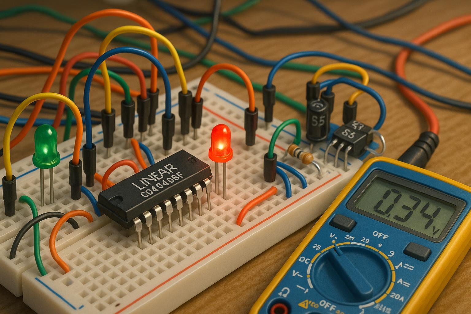
Insert CD4040BF onto breadboard, orient dot/pin 1.
Connect pin 16 (VDD) to +5V, pin 8 (VSS) to GND.
Tip: Place a 0.1µF ceramic capacitor close across VDD and VSS pins for noise immune operation.
Pause & Verify: Confirm power connections with a multimeter before continuing.
Step 2: Hook Up the Clock Input
Build a simple 555 astable circuit or attach your signal generator; output connects to pin 10 (CLK).
Add a 10kΩ pulldown resistor from pin 10 to ground to stabilize input.
From Experience: A clean clock signal is crucial—floating or noisy clocks cause erratic counting!
Pause & Verify: Check clock pulses (scope/multimeter frequency function if available).
Step 3: Configure the Reset Pin
Tie pin 11 (RESET) to ground for normal counting.
Wire a pushbutton between RESET and +5V if you want manual resets; releasing the button should pull back to GND (reset is active HIGH).
Error Prevention: Never leave RESET floating—connect to a defined logic level.
Pause & Verify: Press reset, confirm all outputs clear (LEDs go off).
Step 4: Wire the Outputs
For binary visualization, connect each Q output (Q1: pin 9, Q2: pin 7, ..., Q12: pin 12) through a 330Ω resistor to an LED, then to ground.
You can use only a few LEDs for key outputs if preferred. For digital verification, probe outputs directly.
Tip: LEDs will flicker at a frequency divided by 2ⁿ (Q1: CLK/2, Q2: CLK/4, ... Q12: CLK/4096)
Pause & Verify: Power on, check pattern of LEDs matches expected binary count.
Step 5: Test and Troubleshoot
Apply clock pulses, observe outputs changing in binary sequence.
Use oscilloscope/multimeter frequency function for detailed stage-by-stage checks.
Troubleshooting:
If no counting, recheck clock generator and RESET pin wiring
If erratic counting, ensure clock is debounced and all unused inputs properly grounded
If outputs don't clear, test RESET pin manually
Spot miswiring or swapped pin connections—refer to datasheet pinout
From Experience: Always double-check the pin mapping against the datasheet before powering up!
Common Pitfalls & Solutions
Floating Inputs: Always tie unused pins to GND or VDD
Noisy Clock: Use shielded wires for clock; consider Schmitt trigger buffer
Output Overload: Don't connect outputs directly to high-power loads—buffer outputs if driving external logic
Misreading Outputs: Use LED indicators or digital probe for clear state display
No Decoupling Capacitor: Add one close to the IC power pins to prevent glitches
Extending Your Project
Chaining Multiple CD4040BFs: Cascade outputs for higher bit counts—connect overflow/carry-out to next chip's clock input
Building a Frequency Meter: Use CD4040BF as a front-end divider for an MCU-based frequency measurement circuit
Microcontroller Integration: Read binary state of Q outputs with Arduino, STM32, or similar via parallel port for advanced monitoring
Industrial/Hobby Applications: Designed for reliability from -55°C to 125°C, makes it suitable for serious and DIY uses alike
Reference for advanced use: TI CD4040B Datasheet, 2025
Quick Reference: Division Ratios
Output | Stage | Frequency Division |
|---|---|---|
Q1 | 1 | CLK ÷ 2 |
Q2 | 2 | CLK ÷ 4 |
... | ... | ... |
Q12 | 12 | CLK ÷ 4096 |
Best Practices & Safety Reminders
Use ESD precautions: wrist strap, grounded mat when handling IC
Keep wire/trace lengths short; minimize crosstalk
Don’t exceed voltage or temperature ratings (see datasheet)
Always reference authoritative sources for pinouts and specs
Authoritative Technical Resources
For further questions, peer support, and ongoing experiments, check out:
Instructables: Electronic Counters
From the workbench: If you hit a snag, take a deep breath—most issues are simple connection errors or noisy clocks. With patience and stepwise checks, you'll have your CD4040BF counting reliably in no time!